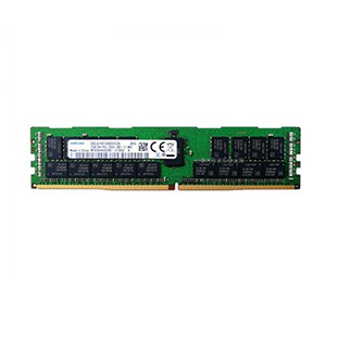
- DDR
- GDDR
- LPDDR
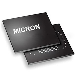
- FLASH
- eMMC
- MCP
- eMCP
- RLDRAM
- UFS
- HBM
- SSD
- RAM
- HDD
- CPU
- GPU
- Wafer
- GPU server
- HOT OFFER
-
OTHER
- MCU
- XILINX
- INTEL
-
TI
- interface
- PMIC-Regulator-Linear
- Data Acquisition - Digital to Analog Converter ADC
- Linear Devices - Amplifiers
- Linear Devices - Voltage Regulators
- MCU
- switch controller
- power management
- DC converter
- voltage reference
- Comparators
- converter
- SENSOR
- driver
- monitor
- LED driver
- logic-signal switch
- Distribution switch
- grid inverter
- OTHER
- SENSOR
-
ONSEMI
- MOSFET
- Schottky diodes
- Rectifier
- AC-DC controller and regulator
- ESD diode
- LED driver
- Optocoupler-phototransistor output
- Monitor and reset the chip
- Switching diode
- Fast recovery/ultrafast recovery diode
- Logic gate
- Transistor
- General purpose diode
- Zener diode
- Linear regulator
- Operational Amplifier
- Gate drive IC
- OTHER
- infineon
- ADI
- ISSI
- MAXIM
- TOSHIBA
- CYPRESS
- NIC
- memory
- Switch

Similar product


Product Detail
产品详情
| 脚位/封装 | TSOP-48 |
| 外包装 | |
| 无铅/环保 | 无铅/环保 |
| 电压(伏) | 3.3 V |
| 温度规格 | 0° ~ 70°C |
| 速度 | 1 MHZ |
| 标准包装数量 | 1000 |
| 标准外箱 | |
| Number Of Words | 2G |
| Bit Organization | x8 |
| Density | 16G |
| Features | Polyimide (if applicable) |
| Package | TSOP I(48-pin CPL version) |
| Generation Feature Set | 3rd set of device features (rev only if different) |
| Speed Grade | Async only |
| Design Revision | C |
| Classification | 1-1-1-1 (Die-nCE-RnB-IO Channels) |
| Level | SLC |
| Production Status | Production |
| Package Material | Pb-free |
| Interface | Async only |
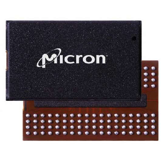
General Description Micron NAND Flash devices include an asynchronous data interface for high-performance I/O operations. These devices use a highly multiplexed 8-bit bus (I/Ox) to transfer commands, address, and data. There are five control signals used to implement the asynchronous data interface: CE#, CLE, ALE, WE#, and RE#. Additional signals control hardware write protection and monitor device status (R/B#). This hardware interface creates a low pin-count device with a standard pinout that remains the same from one density to another, enabling future upgrades to higher densities with no board redesign. A target is the unit of memory accessed by a chip enable signal. A target contains one or more NAND Flash die. A NAND Flash die is the minimum unit that can independently execute commands and report status. A NAND Flash die, in the ONFI specification, is referred to as a logical unit (LUN). There is at least one NAND Flash die per chip enable signal. For further details, see Device and Array Organization.
RECOMMEND


Hot product




Scan QR code and add customer




 MTA32ATF4G64HZ-2G6B2 SODIMM DDR4 MICROM
